
|
| Place of Origin | Call |
| Brand Name | Diodes Incorporated |
| Certification | Lead free / RoHS Compliant |
| Model Number | BSS84-7-F |
Description
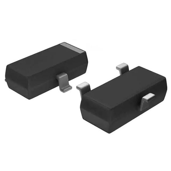
The BSS84-7-F is a P-channel enhancement-mode MOSFET with solderable matte tin plated terminals as per MIL-STD-202 standard. It is designed to minimize the ON-state resistance RDS (ON) and yet maintain superior switching performance, making it ideal for high efficiency power management applications.
Product Summary
Features
Low ON-resistance
Low gate threshold voltage
Low input capacitance
Fast switching speed
Low input/output leakage
Halogen-free, Green device
Moisture sensitivity level 1 as per J-STD-020
UL94V-0 Flammability rating
Mechanical Data
• Case: SOT23 (Standard)
• Case Material: UL Flammability Classification Rating 94V-0 • Moisture Sensitivity: Level 1 per J-STD-020
• Terminals: Matte Tin Finish (Lead Free Plating) Solderable per MIL-STD-202, Method 208
• Terminal Connections: See Diagram
• Weight: 0.009 grams (Approximate)
Maximum Ratings
(@ TA = +25°C, unless otherwise specified.)
| Characteristic | Symbol | Value | Unit |
| Drain-Source Voltage | VDSS | -50 | V |
| Drain-Gate Voltage RGS £ 20kW | VDGR | -50 | V |
| Gate-Source Voltage Continuous | VGSS | ±20 | V |
| Drain Current (Note 5) Continuous | ID | -130 | mA |
| Pulsed Drain Current | IDM | -1.2 | A |
Thermal Characteristics
(@ TA = +25°C, unless otherwise specified.)
| Characteristic | Symbol | Value | Unit |
| Total Power Dissipation (Note 5) | PD | 300 | mW |
| Thermal Resistance, Junction to Ambient | RqJA | 417 | ° C/W |
| Operating and Storage Temperature Range | TJ, TSTG | -55 to +150 | °C |
Electrical Characteristics
(@ TA = +25°C, unless otherwise specified.)
| Characteristic | Symbol | Min | Typ | Max | Unit | Test Condition |
| OFF CHARACTERISTICS (Note 6) | ||||||
| Drain-Source Breakdown Voltage | BVDSS | -50 | ¾ | ¾ | V | VGS = 0V, ID = -250µA |
|
Zero Gate Voltage Drain Current |
IDSS |
¾ ¾ ¾ |
¾ ¾ ¾ |
-1 -2 -100 |
µA µA nA | VDS = -50V, VGS = 0V, TJ = +25°C VDS = -50V, VGS = 0V, TJ = +125°C VDS = -25V, VGS = 0V, TJ = +25°C |
| Gate-Body Leakage | IGSS | ¾ | ¾ | ±10 | nA | VGS = ±20V, VDS = 0V |
| ON CHARACTERISTICS (Note 6) | ||||||
| Gate Threshold Voltage | VGS(th) | -0.8 | ¾ | -2.0 | V | VDS = VGS, ID = -1mA |
| Static Drain-Source On-Resistance | RDS(on) | ¾ | 3.2 | 10 | W | VGS = -5V, ID = -0.100A |
| Forward Transconductance | gFS | 0.05 | ¾ | ¾ | S | VDS = -25V, ID = -0.1A |
| DYNAMIC CHARACTERISTICS (Note 7) | ||||||
| Input Capacitance | Ciss | ¾ | 24.6 | 45 | pF |
VDS = -25V, VGS = 0V, f = 1.0MHz |
| Output Capacitance | Coss | ¾ | 4.7 | 25 | pF | |
| Reverse Transfer Capacitance | Crss | ¾ | 2.8 | 12 | pF | |
| Gate Resistance | Rg | ¾ | 916 | ¾ | Ω | VDS = 0V, VGS = 0V, f = 1MHz |
| Total Gate Charge (VGS = -4.5V) | Qg | ¾ | 0.28 | ¾ | nC |
VDS = -10V, ID = -0.1A |
| Total Gate Charge (VGS = -10V) | Qg | ¾ | 0.59 | ¾ | nC | |
| Gate-Source Charge | Qgs | ¾ | 0.09 | ¾ | nC | |
| Gate-Drain Charge | Qgd | ¾ | 0.08 | ¾ | nC | |
| Turn-On Delay Time | tD(on) | ¾ | 10 | ¾ | ns | VDD = -30V, ID = -0.27A, RGEN = 50Ω, VGS = -10V |
| Turn-Off Delay Time | tD(off) | ¾ | 18 | ¾ | ns | |
![]()
![]()
Package Outline Dimensions
![]()
Suggested Pad Layout
![]()
Datasheet
You can download the datasheet the link given below.
![]()
Contact Us at Any Time


