
|
| Place of Origin | Call |
| Brand Name | Cypress Semiconductor |
| Certification | Lead free / RoHS Compliant |
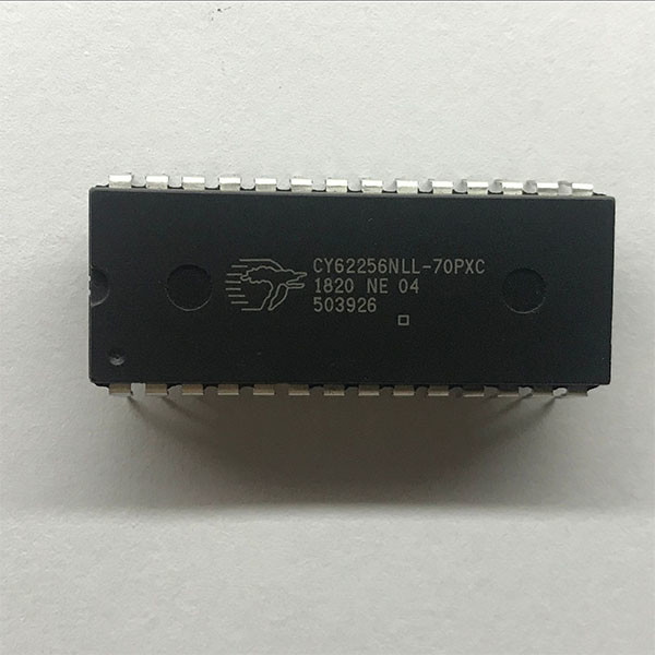
| Model Number | CY62256NLL-70PXC |
Description
The CY62256N is a high performance CMOS static RAM organized as 32K words by 8 bits. Easy memory expansion is provided by an active LOW chip enable (CE) and active LOW output enable (OE) and tristate drivers. This device has an automatic power-down feature, reducing the power consumption by 99.9 percent when deselected.
An active LOW write enable signal (WE) controls the writing/reading operation of the memory. When CE and WE inputs are both LOW, data on the eight data input/output pins (I/O0 through I/O7) is written into the memory location addressed by the address present on the address pins (A0 through A14).
Reading the device is accomplished by selecting the device and enabling the outputs, CE and OE active LOW, while WE remains inactive or HIGH. Under these conditions, the contents of the location addressed by the information on address pins are present on the eight data input/output pins.
The input/output pins remain in a high impedance state unless the chip is selected, outputs are enabled, and write enable (WE) is HIGH.
Pin Configuration
![]()
CY62256NLL-70PXC Logic Block Diagram
![]()
CY62256NLL-70PXC Features
■ Temperature ranges
❐ Commercial: 0 °C to +70 °C
❐ Industrial: –40 °C to +85 °C
❐ Automotive-A: –40 °C to +85 °C
❐ Automotive-E: –40 °C to +125 °C
■ High speed: 55 ns
■ Voltage range: 4.5 V to 5.5 V operation
■ Low active power
❐ 275 mW (max)
■ Low standby power (LL version)
❐ 82.5 mW (max)
■ Easy memory expansion with CE and OE Features
■ TTL-compatible inputs and outputs
■ Automatic power-down when deselected
■ CMOS for optimum speed and power
■ Available in Pb-free and non Pb-free 28-pin (600-mil) PDIP,
28-pin (300-mil) narrow SOIC, 28-pin TSOP I, and 28-pin
reverse TSOP I packages
CY62256NLL-70PXC Maximum Ratings
Exceeding maximum ratings may impair the useful life of the device. These user guidelines are not tested.
Storage temperature ................................ –65℃ to +150℃
Ambient temperature with power applied .......................................... –55℃ to +125℃
Supply voltage to ground potential(pin 28 to pin 14) .....................................–0.5 V to +7.0 V
DC voltage applied to outputs in high Z State ................................ -0.5 V to VCC + 0.5 V
DC input voltage ............................. –0.5 V to VCC + 0.5 V
Datasheet
You can download the datasheet the link given below.
![]()
Contact Us at Any Time


