
 Home
>
PRODUCTS
>
Semiconductor ICs
>
Home
>
PRODUCTS
>
Semiconductor ICs
>
|
| Place of Origin | Call |
| Brand Name | Intel / Altera |
| Certification | ROHS |
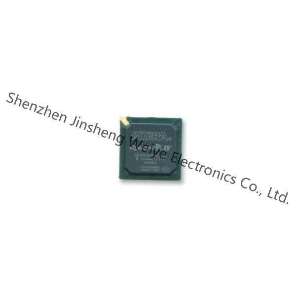
| Model Number | EP2S30F484C3N |
[Altera]
The Stratix® II FPGA family is based on a 1.2-V, 90-nm, all-layer copper SRAM process and features a new logic structure that maximizes performance, and enables device densities approaching 180,000 equivalent logic elements (LEs). Stratix II devices offer up to 9 Mbits of on-chip, TriMatrix™ memory for demanding, memory intensive applications and has up to 96 DSP blocks with up to 384 (18-bit × 18-bit) multipliers for efficient implementation of high performance filters and other DSP functions.
The Stratix II family offers the following features:
■ 15,600 to 179,400 equivalent LEs; see Table 1–1
■ New and innovative adaptive logic module (ALM), the basic building block of the Stratix II architecture, maximizes performance and resource usage efficiency
■ Up to 9,383,040 RAM bits (1,172,880 bytes) available without reducing logic resources
■ TriMatrix memory consisting of three RAM block sizes to implement true dual-port memory and first-in first-out (FIFO) buffers
■ High-speed DSP blocks provide dedicated implementation of multipliers (at up to 450 MHz), multiply-accumulate functions, and finite impulse response (FIR) filters
■ Up to 16 global clocks with 24 clocking resources per device region
■ Clock control blocks support dynamic clock network enable/disable, which allows clock networks to power down to reduce power consumption in user mode
■ Up to 12 PLLs (four enhanced PLLs and eight fast PLLs) per device provide spread spectrum, programmable bandwidth, clock switchover, real-time PLL reconfiguration, and advanced multiplication and phase shifting
■ Support for numerous single-ended and differential I/O standards
■ High-speed differential I/O support with DPA circuitry for 1-Gbps performance
■ Support for high-speed networking and communications bus standards including Parallel RapidIO, SPI-4 Phase 2 (POS-PHY Level 4), HyperTransport™ technology, and SFI-4
■ Support for high-speed external memory, including DDR and DDR2 SDRAM, RLDRAM II, QDR II SRAM, and SDR SDRAM
■ Support for multiple intellectual property megafunctions from Altera MegaCore® functions and Altera Megafunction Partners Program (AMPPSM) megafunctions
■ Support for design security using configuration bitstream encryption
■ Support for remote configuration updates
Specifications
| Attribute | Attribute Value |
|---|---|
| Manufacturer | Intel / Altera |
| Product Category | FPGAs (Field Programmable Gate Array) |
| Series | Stratix® II |
| Product | Stratix II |
| Packaging | Tray |
| Mounting-Style | SMD/SMT |
| Tradename | Stratix II |
| Package-Case | 484-BBGA, FCBGA |
| Operating-Temperature | 0°C ~ 85°C (TJ) |
| Mounting-Type | Surface Mount |
| Voltage-Supply | 1.15 V ~ 1.25 V |
| Supplier-Device-Package | 484-FBGA (23x23) |
| IC Number of Gates | - |
| Number-of-I-O | 342 I/O |
| Number-of-LABs-CLBs | 1694 |
| Number-of-Logic-Elements-Cells | 33880 |
| Total-RAM-Bits | 1369728 Bits |
| Maximum Operating Temperature | + 70 C |
| Operating temperature range | 0 C |
| Operating-Supply-Voltage | 1.2 V |
| Operating-Supply-Current | 0.3 A |
| Package-Case | FBGA-484 |
| Input/output | 342 I/O |
| Number-of-Logic-Array-Blocks-LABs | 1694 |
| Number-of-Logic-Elements | 33880 Logic Elements |
| Total-Memory | 1369728 bit |
Form,Package,Functional compatible component
Descriptions
Who we are?
is a professional electronic marketing corporation entirely engaged in the fields of semi-conductors and electronic components sale and service for clients over 10 years, specialize in selling the new and unused, original factory sealed packing electronic components. specialize in IC,diode,transistor,IGBT,DC-DC converter.....***has set up our own sales service conception and has already established strong partnerships with many famous manufacturers and we have more than 5,000,000 kinds of electronic components for your choices, always at your services !
FAQ
Q: Are you trading company or manufacturer?
A: We are original manufacturer OF Integrated Circuit Chip . We can do OEM/ODM business.
Q: How long is your delivery time?
A: Group buying delivery time: 30-60 days; General delivery time: 20 days.
Q: What is your terms of payment?
A: T/T 30% as deposit, and 70% before delivery.
Q: How to buy your products?
A: You can buy the products from our company directly.Normally the procedure is sign the contract, payment by T/T,Contact the shipping company to delivery the goods to your country.Q: What is the warranty ?
A: The free warranty is one year from the day of Commissioning qualified.If there is any fault for our products within the free warranty period, we will repair it and change the fault assembly for free
Contact Us at Any Time

