
 Home
>
PRODUCTS
>
Semiconductor ICs
>
Home
>
PRODUCTS
>
Semiconductor ICs
>
|
| Place of Origin | Call |
| Brand Name | Freescale / NXP |
| Certification | ROHS |
| Model Number | MC908GR32ACFAE |
Product Details
Introduction
The MC68HC908GR60A, MC68HC908GR48A, and MC68HC908GR32A are members of the low-cost, high-performance M68HC08 Family of 8-bit microcontroller units (MCUs). All MCUs in the family use the enhanced M68HC08 central processor unit (CPU08) and are available with a variety of modules, memory sizes and types, and package types.
For convenience, features have been organized to reflect:
• Standard features
• Features of the CPU08
Features of the MC68HC908GR60A include:
• High-performance M68HC08 architecture optimized for C-compilers
• Fully upward-compatible object code with M6805, M146805, and M68HC05 Families
• 8-MHz internal bus frequency
• Clock generation module supporting 1-MHz to 8-MHz crystals
• FLASH program memory security(1)
• On-chip programming firmware for use with host personal computer which does not require high voltage for entry
• In-system programming (ISP)
• System protection features:
– Optional computer operating properly (COP) reset
– Low-voltage detection with optional reset and selectable trip points for 3.3-V and 5.0-V operation
– Illegal opcode detection with reset
– Illegal address detection with reset
• Low-power design; fully static with stop and wait modes
• Standard low-power modes of operation:
– Wait mode
– Stop mode
• Master reset pin and power-on reset (POR)
• On-chip FLASH memory:
– MC68HC908GR60A — 60 Kbytes
– MC68HC908GR48A — 48 Kbytes
– MC68HC908GR32A — 32 Kbytes
• Random-access memory (RAM):
– MC68HC908GR60A — 2048 bytes
– MC68HC908GR48A — 1536 bytes
– MC68HC908GR32A — 1536 bytes
• Serial peripheral interface (SPI) module
• Enhanced serial communications interface (ESCI) module
• One 16-bit, 2-channel timer interface module (TIM1) with selectable input capture, output compare, and pulse-width modulation (PWM) capability on each channel
• One 16-bit, 6-channel timer interface module (TIM2) with selectable input capture, output compare, and pulse-width modulation (PWM) capability on each channel
• Timebase module with clock prescaler circuitry for eight user selectable periodic real-time interrupts with optional active clock source during stop mode for periodic wakeup from stop using an external crystal
• 24-channel, 10-bit successive approximation analog-to-digital converter (ADC)
• 8-bit keyboard wakeup port with software selectable rising or falling edge detect, as well as high or low level detection
• Up to 53 general-purpose input/output (I/O) pins, including:
– 40 shared-function I/O pins, depending on package choice
– Up to 13 dedicated I/O pins, depending on package choice
• Selectable pullups on inputs only on ports A, C, and D. Selection is on an individual port bit basis. During output mode, pullups are disengaged.
• Internal pullups on IRQ and RST to reduce customer system cost
• High current 10-mA sink/source capability on all port pins
• Higher current 20-mA sink/source capability on PTC0–PTC4 and PTF0–PTF3
• User selectable clockout feature with divide by 1, 2, and 4 of the bus or crystal frequency
• User selection of having the oscillator enabled or disabled during stop mode
• BREAK module (BRK) to allow single breakpoint setting during in-circuit debugging
• Available packages:
– 32-pin low-profile quad flat pack (LQFP)
– 48-pin low-profile quad flat pack (LQFP)
– 64-pin quad flat pack (QFP)
• Specific features in 32-pin LQFP are:
– Port A is only 4 bits: PTA0–PTA3; shared with ADC and KBI modules
– Port B is only 6 bits: PTB0–PTB5; shared with ADC module
– Port C is only 2 bits: PTC0–PTC1
– Port D is only 7 bits: PTD0–PTD6; shared with SPI, TIM1 and TIM2 modules
– Port E is only 2 bits: PTE0–PTE1; shared with ESCI module
Specifications
| Attribute | Attribute Value |
|---|---|
| Manufacturer | Freescale / NXP |
| Product Category | Microcontrollers |
| Series | HC08 |
| Packaging | Tray |
| Unit-Weight | 0.006288 oz |
| Mounting-Style | SMD/SMT |
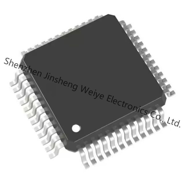
| Package-Case | 48-LQFP |
| Operating-Temperature | -40°C ~ 85°C (TA) |
| Supplier-Device-Package | 48-LQFP (7x7) |
| Number-of-I-O | 37 I/O |
| Speed | 8MHz |
| EEPROM-Size | - |
| Core-Processor | HC08 |
| RAM-Size | 1.5K x 8 |
| Program Memory | FLASH |
| Peripherals | LVD, POR, PWM |
| Connectivity | SCI, SPI |
| Voltage-Supply-Vcc-Vdd | 3 V ~ 5.5 V |
| Core-Size | 8-Bit |
| Program-Memory-Size | 32KB (32K x 8) |
| Data-Converters | A/D 24x10b |
| Oscillator-Type | Internal |
| Maximum Operating Temperature | + 85 C |
| Operating temperature range | - 40 C |
| Interface-Type | ESCI SPI |
| Core | HC08 |
| Processor-Series | HC08GR |
| Data-Bus-Width | 8 bit |
| Supply-Voltage-Max | 5.5 V |
| Supply-Voltage-Min | 2.97 V |
| Package-Case | LQFP-48 |
| Maximum-Clock-Frequency | 8 MHz |
| Number-of-ADC-Channels | 24 ADC Channels |
| Input/output | 53 I/O |
| Data-RAM-Size | 1.5 kB |
|
Number-of-Timers-Counters |
8 Timer |
| ADC-Resolution | 10 bit |
Who we are?
FAQ
Q: Are you trading company or manufacturer?
A: We are original manufacturer OF Integrated Circuit Chip . We can do OEM/ODM business.
Q: How long is your delivery time?
A: Group buying delivery time: 30-60 days; General delivery time: 20 days.
Q: What is your terms of payment?
A: T/T 30% as deposit, and 70% before delivery.
Q: How to buy your products?
A: You can buy the products from our company directly.Normally the procedure is sign the contract, payment by T/T,Contact the shipping company to delivery the goods to your country.
Q: What is the warranty ?
A: The free warranty is one year from the day of Commissioning qualified.If there is any fault for our products within the free warranty period, we will repair it and change the fault assembly for free.
6-TSSOP,
Contact Us at Any Time

